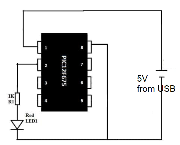
Analog reading made easy. Today we will configure and use analog input with PIC12F675 and MPLAB X, showing analog value (voltage) in two LED that will blink accordingly. While doing my research for this article (which I will use as part of a thermometer keychain project), I figured exists almost no examples of analog input reading with PIC12F675 on the internet. Today we are changing that.
According to the 12F675 dasheet, it features four analog channels (pins 3, 5, 6 and 7) with 10bit resolution, delivering 0-5V readings (when the chip is supplied with 5V) to 0-1023 integers. Readings are supplied in binary format at ADRESH (2 highest bits) and ADRESL (8 lowest bits) – this is selectable (you can have ADRESH be the higher or the lower bits).
The circuit
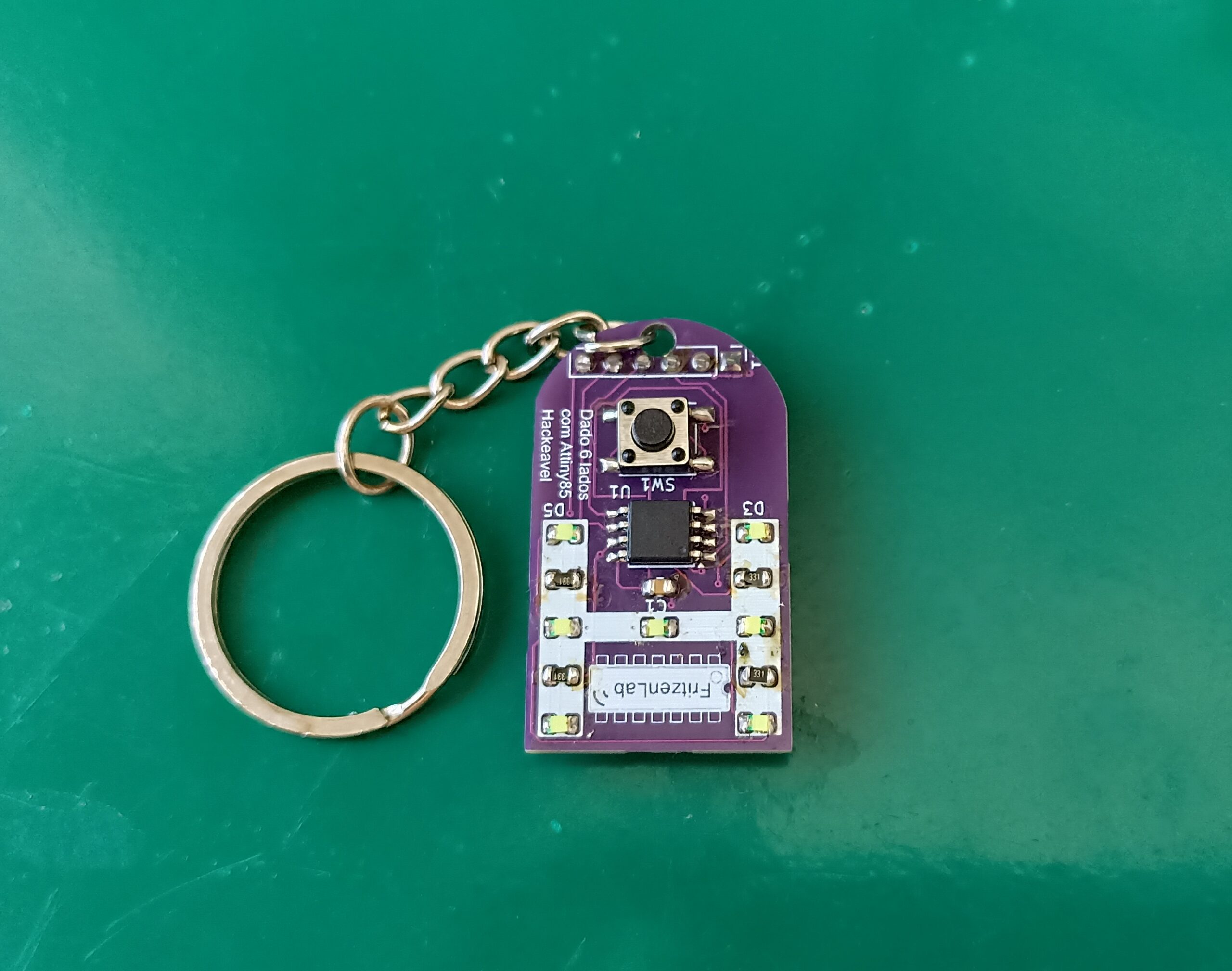
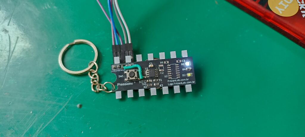
For testing purposes I will be implementing the analog readings in two channels: NTC thermistor in AN2 and resistor divider in AN3, as seen below. This is due to the fact that I am using my “FritzenLab keychain” circuit board for testing and development. This keychain will feature a thermometer with said NTC and two LEDs.
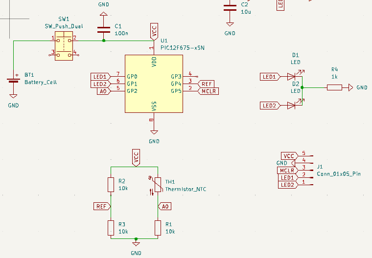
Notice the termistor circuit connected to GP2, resistor divider connected to GP4 and two LEDs, connected to GP0 and GP1.
Coding
In this tutorial (Analog reading made easy) I am using MPLAB X as the IDE, XC8 as the compiler and PICkit3 as the programmer, as configured here and here. Code was adapted from these sources: here and here.
First thing we have to do is configure all necessary registers for both analog input and digital outputs. Amongst the most important is TRISIO to define GP2 and GP4 as inputs, other pins outputs:
TRISIO = 0b010100;// GP2 and GP4 analog inputsThen we communicate ANSEL that AN2 and AN3 are going to be used as analog:
ANSEL = 0b00011100;// AN2 and AN3 as analog inputsAlso ADCON0 for general analog configurations (in this case for AN3):
ADCON0=0b10001101; // AN3, right justified, VDD as refNow for AN2 (commented for now, not using it):
//ADCON0=0b00001001; // AN2, right justified, VDD as refFinally enabling the ADC module:
ADON=1; // Enable ADCNow we have to execute analog readings. For that I decide to do it periodically, using an interrupt of Timer0: it is configured to enter the interrupt function every ~65ms (milisseconds) (4MHz internal oscillator, being divided by 4 and with a 256 prescaler). Despite entering the interrupt every ~65ms I only enter my code every 4x that (so around 260ms).
I then have an IF with two ELSEs: IF “readAndDecide” is true (if it is time to make an analog reading) it does just that then proceeds (in the next cycle) to the first ELSE, which controls the tens LED. Tens LED will blink the number of times of the most significant digit: if for example the analog voltage read is 3.7V, tens LED will blink 3 times.
Then the first ELSE handles control to the second ELSE, which blinks the number of times the units analog read was made. In the example above if the voltage read was 3.7V, the units LED will blink 7 times. So for example if the voltage read in the IF was 1.2V, tens LED will blink once and unit LED will blink twice, and so on.
After both LEDs blink (first the tens then the units) the control is handled back to the main IF which will make another analog read. It keeps going forever. Complete code is below and also in my Github.
/*
 Timer based on this code: https://microcontroladores-c.blogspot.com/2014/09/timer0-com-pic12f675.html
 * AD converter based on: https://forum.microchip.com/s/topic/a5C3l000000MRbeEAG/t336178
 * AD code also from here: https://saeedsolutions.blogspot.com/2012/07/pic12f675-adc-code-proteus-simulation.html
 */
#include <stdio.h>
#include <stdlib.h>
#include <xc.h>
#include <math.h>
#define _XTAL_FREQ 4000000

#define LED1 GP0
#define LED2 GP1
/////////////////////////////////////////////////////////configuraçôes//////////////////////////////////////////////////
#pragma config FOSC = INTRCIO   // Oscillator Selection bits (INTOSC oscillator: I/O function on GP4/OSC2/CLKOUT pin, I/O function on GP5/OSC1/CLKIN)
#pragma config WDTE = OFF       // Watchdog Timer Enable bit (WDT disabled)
#pragma config PWRTE = ON       // Power-Up Timer Enable bit (PWRT enabled)
#pragma config MCLRE = OFF      // GP3/MCLR pin function select (GP3/MCLR pin function is digital I/O, MCLR internally tied to VDD)
#pragma config BOREN = OFF      // Brown-out Detect Enable bit (BOD disabled)
#pragma config CP = OFF         // Code Protection bit (Program Memory code protection is disabled)
#pragma config CPD = OFF         // Data Code Protection bit (Data memory code protection is enabled)


volatile uint8_t counter= 0;
volatile int reading= 0;
volatile unsigned int voltage= 0;
volatile uint8_t readAndDecide= 1;
volatile int tens= 0;
volatile int units= 0;
volatile uint8_t executeTens= 0;
volatile uint8_t executeUnits= 0;

void __interrupt() isr()//interrupt vector
{
    counter++;
    if(counter == 4){
        counter= 0;

        if(readAndDecide == 1){
            readAndDecide= 0;
            executeTens= 1;
            executeUnits= 0;

            GO_nDONE= 1;
            while(GO_nDONE);
            reading = ((ADRESH<<8)+ADRESL);
            voltage = (reading * 50) / 1024; // 0-50 instead of 0-5 (v))

            if(voltage >= 40){
            tens= 4;
            units= voltage - 40;
            }else if(voltage >= 30){
                tens= 3;
                units= voltage - 30;
            }else if(voltage >= 20){
                tens= 2;
                units= voltage - 20;
            }else if(voltage >= 10){
                tens= 1;
                units= voltage - 10;
            }else{
                tens= 0;
                units= voltage;
            }
            tens= tens * 2;
            units= units * 2;
        }else if(executeTens == 1){
            tens--;
            LED2= 0;
            if(LED1){
                LED1= 0;
            }else{
                LED1= 1;
            }
            if(tens < 1){
                executeTens= 0;
                executeUnits= 1;
            }

        }else if(executeUnits == 1){
            LED1= 0;
            units--;
            if(LED2){
                LED2= 0;
            }else{
                LED2= 1;
            }
            if(units < 1){
                executeTens= 0;
                executeUnits= 0;
                readAndDecide= 1;
            }

        }


    }

    TMR0IF = 0;//  clear timer0 interrupt flag
    TMR0 = 0;// zeroes timer 0 counting, so that it couts from 256 down to 0 again
}


//////////////////////////////////////////////////////Main routine///////////////////////////////////////////////////////////////
void main(void) {
    TRISIO = 0b010100;// GP2 and GP4 analog inputs
    CMCON = 7;// disable comparators
    ANSEL = 0b00011100;// AN2 and AN3 as analog inputs
    //ADCON0=0b00001001; // AN2, right justified, VDD as ref
    ADCON0=0b10001101; // AN3, right justified, VDD as ref
    ADON=1; // Enable ADC
    WPU = 0X00;// pull ups disabled
    TMR0 = 0;
    OSCCAL = 0b11111111;// internal oscillator to max frequency
    OPTION_REG = 0b10000111;
    INTCON = 0b11100000;


    while(1)
    {


    }//infinite loop

}
Nothing happens in the main loop after it reaches the while(1), all magic is happening in the interrupt handling function. Also please note that in the way I made the code, only one analog input is read at a time. If you want to change to the other you have to uncomment it, comment the other and reflash the PIC12F675.
ADCON0=0b00001001; // AN2, right justified, VDD as ref

OR

ADCON0=0b10001101; // AN3, right justified, VDD as ref

NOT both.
Testing
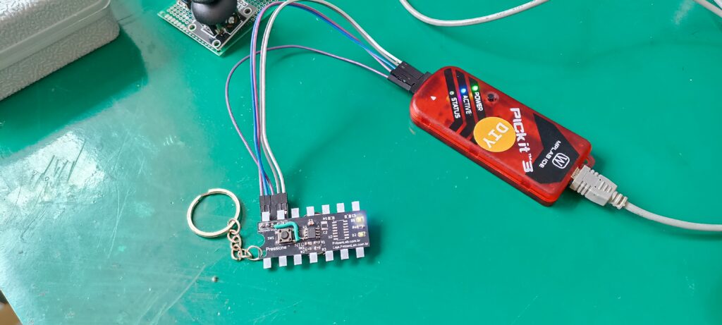
Test setup is pictured above, the keychain connected to PICkit3 and MPLAB X + XC8. I made a video to illustrate all steps necessary to read an analog value with PIC12F675.
